- 您现在的位置:买卖IC网 > Sheet目录1999 > ICS94201DFLF (IDT, Integrated Device Technology Inc)IC FREQ GENERATOR PROGR 56-SSOP
14
ICS94201
0428B - 11/28/05
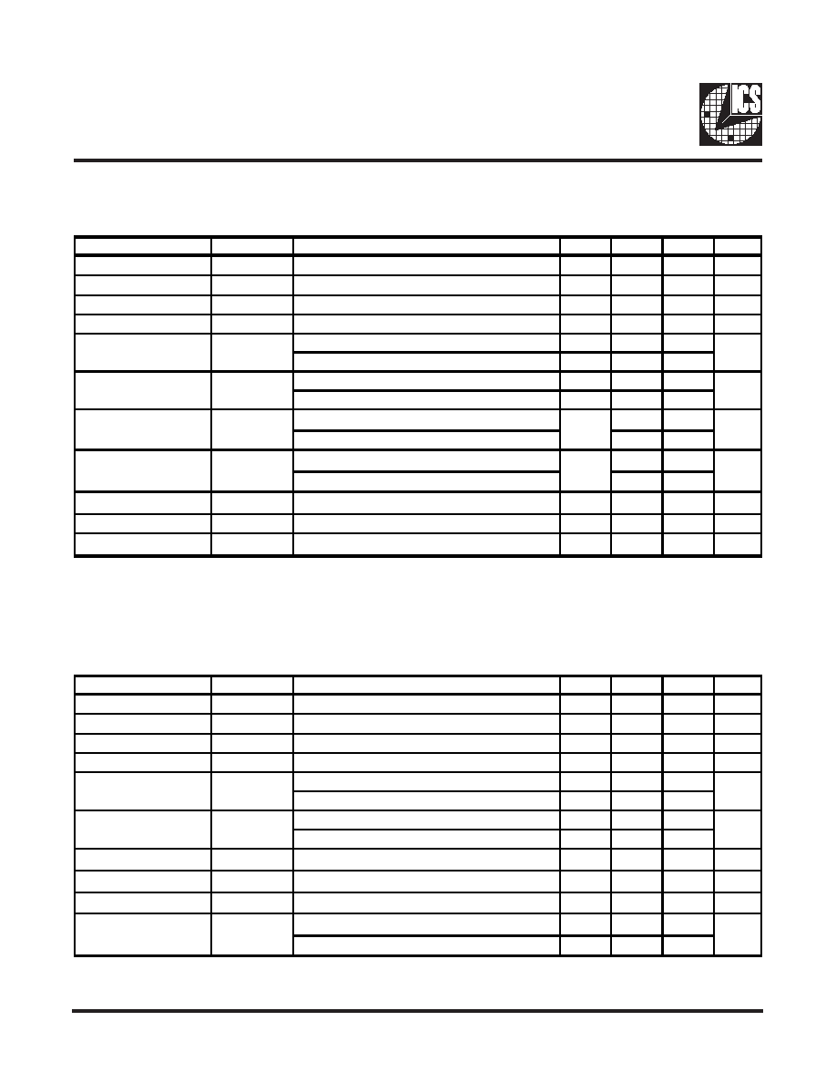
Electrical Characteristics - PCI
TA = 0 - 70 C; VDD = 3.3 V +/-5%, CL = 40 pF for PCI0-1, CL = 10 - 30 pF for other PCIs (unless otherwise stated)
PARAMETER
SYMBOL
CONDITIONS
MIN
TYP
MAX
UNITS
Output Impedance
1
RDSP1
Vo=VDD*(0.5)
12
55
Output Impedance
1
RDSN1
Vo=VDD*(0.5)
12
55
Output High Voltage
VOH1
IOH = -1 mA
2.4
V
Output Low Voltage
VOL1
IOL = 1 mA
0.55
V
VOH@MIN = 1 V
-33
VOH@MAX = 3.135V
-33
VOL@MIN = 1.95 V
30
VOL@MAX =0.4V
38
VOL = 0.4 V, VOH = 2.4 V, PCI0-3
1.8
2
PCI3-7
2.2
2.5
VOL = 2.4 V, VOH = 0.4 V, PCI0-3
1.8
2
PCI3-7
2.3
2.5
Duty Cycle
1
dt1
VT = 1.5 V
45
51
55
%
Skew
1
tsk1
VT = 1.5 V
150
500
ps
Jitter, cycle-to-cycle
1
tjcyc-cyc1
VT = 1.5 V
200
500
ps
1Guaranteed by design, not 100% tested in production.
mA
Output High Current
IOH1
Output Low Current
IOL1
tr1
Rise Time
1
Fall Time
1
tf1
ns
0.5
Electrical Characteristics - REF, 24_48MHz, 48MHz
TA = 0 - 70C; VDD = 3.3 V +/-5%; CL = 10-20 pF (unless otherwise specified)
PARAMETER
SYMBOL
CONDITIONS
MIN
TYP
MAX
UNITS
Output Impedance
1
RDSP5
VO = VDD*(0.5)
20
60
Output Impedance
1
RDSN5
VO = VDD*(0.5)
20
60
Output High Voltage
VOH5
IOH = -1 mA
2.4
V
Output Low Voltage
VOL5
IOL = 1 mA
0.4
V
VOH @ MIN = 1.0 V
-23
VOH @ MAX = 3.135 V
-29
VOL @ MIN = 1.95 V
29
VOL @ MAX = 0.4 V
27
Rise Time
1
tr5
VOL = 0.4 V, VOH = 2.4 V
0.4
2
4
ns
Fall Time
1
tf5
VOH = 2.4 V, VOL = 0.4 V
0.4
2
4
ns
Duty Cycle
1
dt5
VT = 1.5 V
45
53
55
%
VT = 1.5 V, Fixed clocks
200
500
VT = 1.5 V, Ref clocks
2300
3000
1Guaranteed by design, not 100% tested in production.
Jitter, cycle-to-cycle
1
tjcyc-cyc5
ps
Output High Current
IOH5
mA
Output Low Current
IOL5
mA
发布紧急采购,3分钟左右您将得到回复。
相关PDF资料
ICS950218AF
IC TIMING CTRL HUB P4 48-SSOP
ICS950908BFLF
IC TIMING CTRL HUB P4 56-SSOP
ICS951402AGLF
IC TIMING CTRL HUB P4 48-TSSOP
ICS95V847AGIT
IC CLOCK DRIVER 2.5V 24-TSSOP
ICS95V850AGT
IC CLK DVR PLL 1:10 48TSSOP
ICS95V857ALT
IC CLK DVR PLL 1:10 40TVSOP
ICS95V857CKLF8
IC CLK DVR PLL 1:10 40VFQFN
ICS97U870AKT
IC CLK DVR PLL 1:10 40VFQFN
相关代理商/技术参数
ICS94201DFLFT
功能描述:IC FREQ GENERATOR PROGR 56-SSOP RoHS:是 类别:集成电路 (IC) >> 时钟/计时 - 专用 系列:- 标准包装:1,500 系列:- 类型:时钟缓冲器/驱动器 PLL:是 主要目的:- 输入:- 输出:- 电路数:- 比率 - 输入:输出:- 差分 - 输入:输出:- 频率 - 最大:- 电源电压:3.3V 工作温度:0°C ~ 70°C 安装类型:表面贴装 封装/外壳:28-SSOP(0.209",5.30mm 宽) 供应商设备封装:28-SSOP 包装:带卷 (TR) 其它名称:93786AFT
ICS94201DFT
功能描述:IC FREQ GENERATOR PROGR 56-SSOP RoHS:否 类别:集成电路 (IC) >> 时钟/计时 - 专用 系列:- 标准包装:1,500 系列:- 类型:时钟缓冲器/驱动器 PLL:是 主要目的:- 输入:- 输出:- 电路数:- 比率 - 输入:输出:- 差分 - 输入:输出:- 频率 - 最大:- 电源电压:3.3V 工作温度:0°C ~ 70°C 安装类型:表面贴装 封装/外壳:28-SSOP(0.209",5.30mm 宽) 供应商设备封装:28-SSOP 包装:带卷 (TR) 其它名称:93786AFT
ICS94201YFT
制造商:ICS 制造商全称:ICS 功能描述:Programmable System Frequency Generator for PII/III⑩
ICS94203
制造商:ICS 制造商全称:ICS 功能描述:Programmable System Frequency Generator for PII/III⑩
ICS94203F-T
制造商:ICS 制造商全称:ICS 功能描述:Peripheral IC
ICS94203YF-T
制造商:ICS 制造商全称:ICS 功能描述:Programmable System Frequency Generator for PII/III⑩
ICS94206
制造商:ICS 制造商全称:ICS 功能描述:Programmable System Frequency Generator for PII/III⑩
ICS94206YF-T
制造商:ICS 制造商全称:ICS 功能描述:Programmable System Frequency Generator for PII/III⑩